Lithography
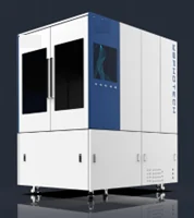
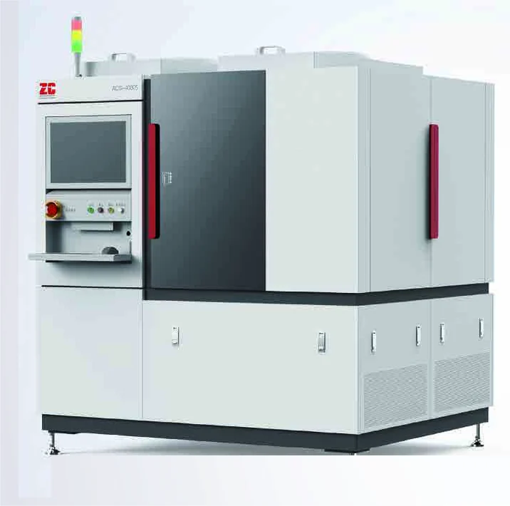
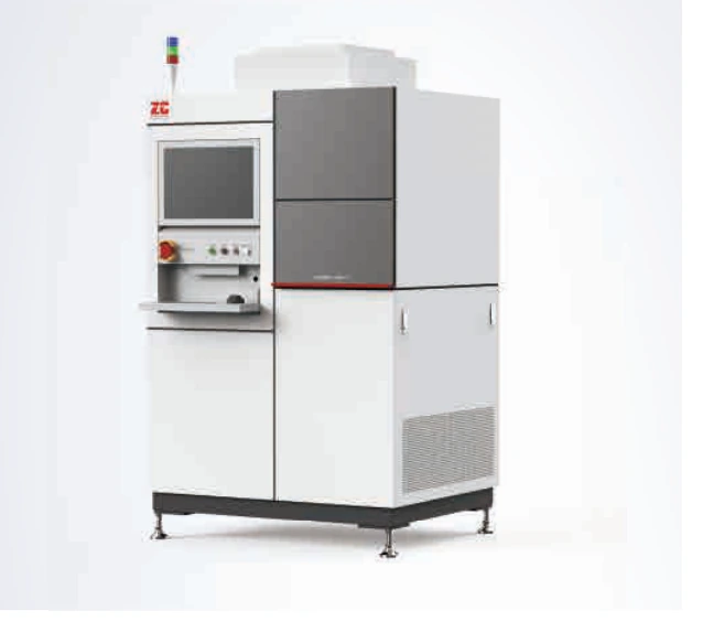
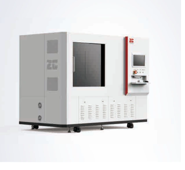
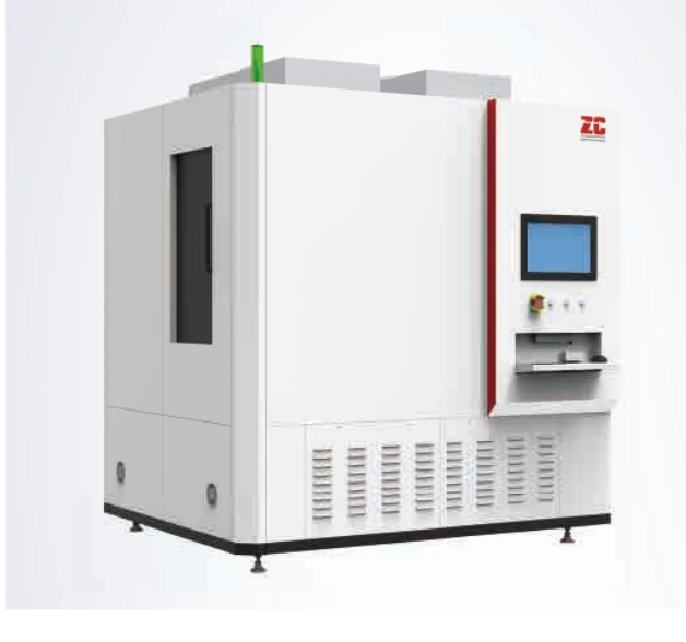
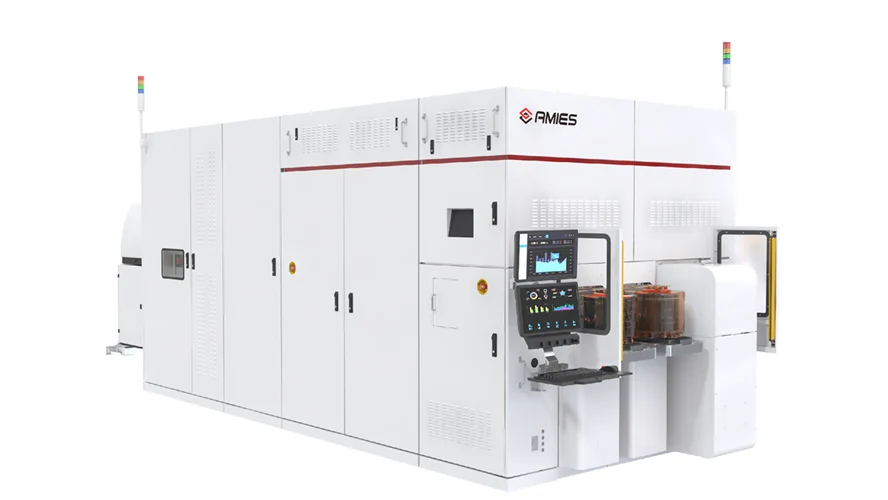
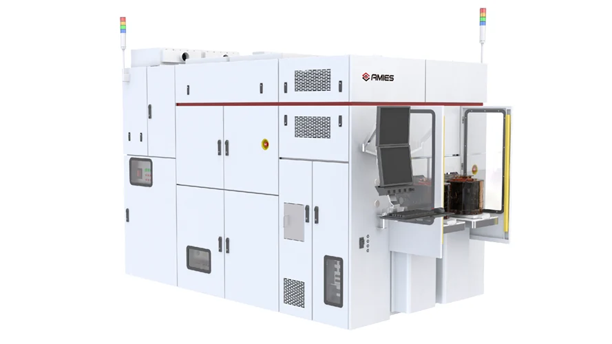
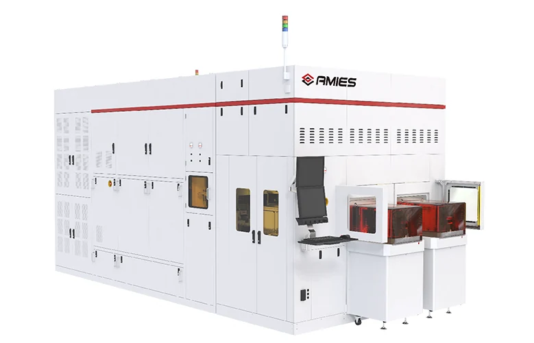
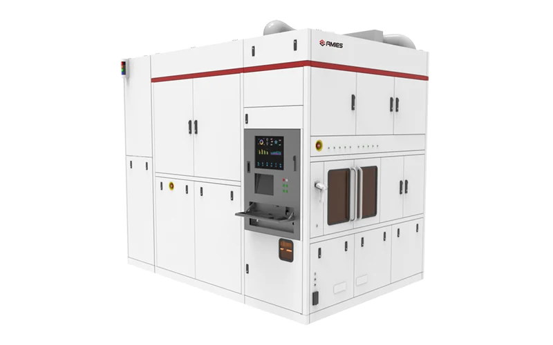
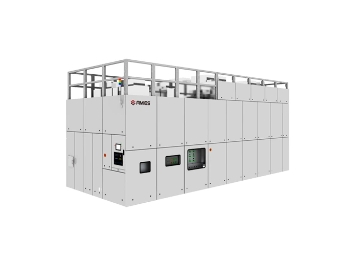
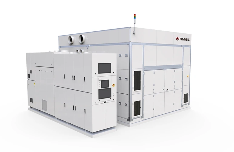
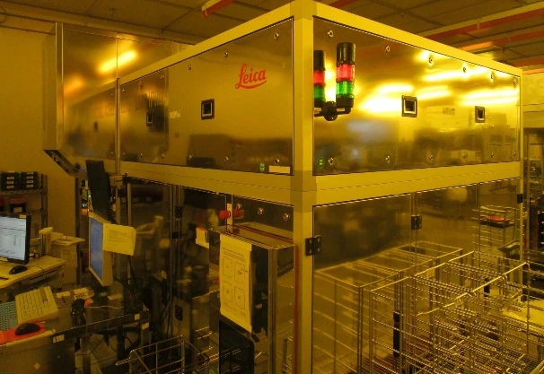
LP3000 Direct-Write Lithography System
Laser direct writing for photomasks, wafers and microfabrication applications.
View productExplore lithography, wafer inspection, optical metrology and automation systems. Select a product to review reference specifications and enquire.
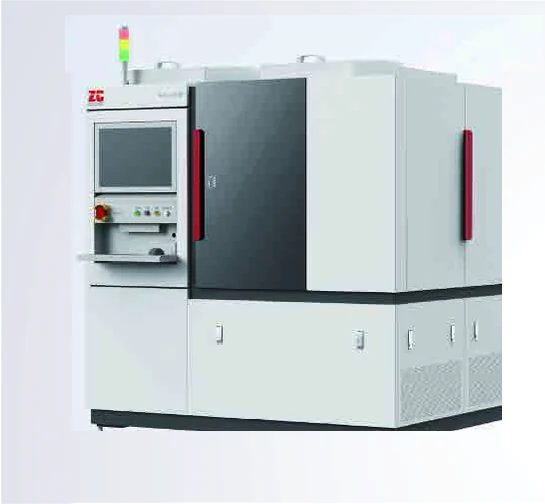
Laser direct writing for photomasks, wafers and microfabrication applications.
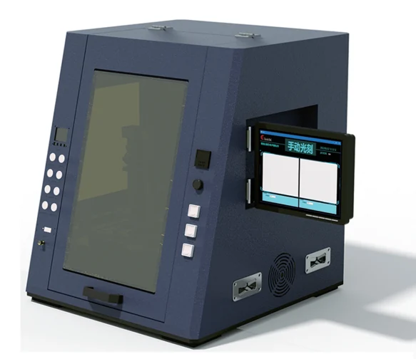
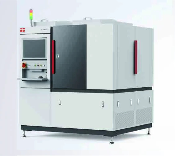
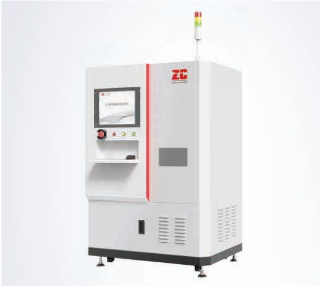
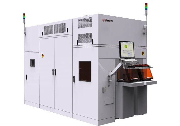
View productMaskless exposure for research, prototyping and small-batch wafer processing.
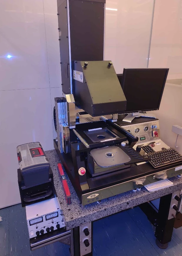
View productManual contact lithography with UV LED illumination for small substrates.
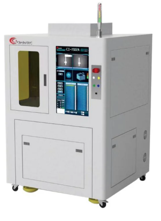
View productAutomatic mask alignment and exposure for 150 mm and 200 mm wafers.
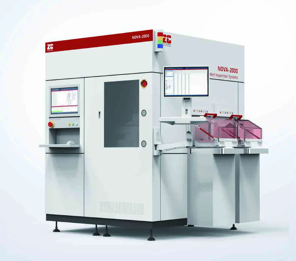
View productOptical defect inspection for polished and epitaxial silicon carbide wafers.
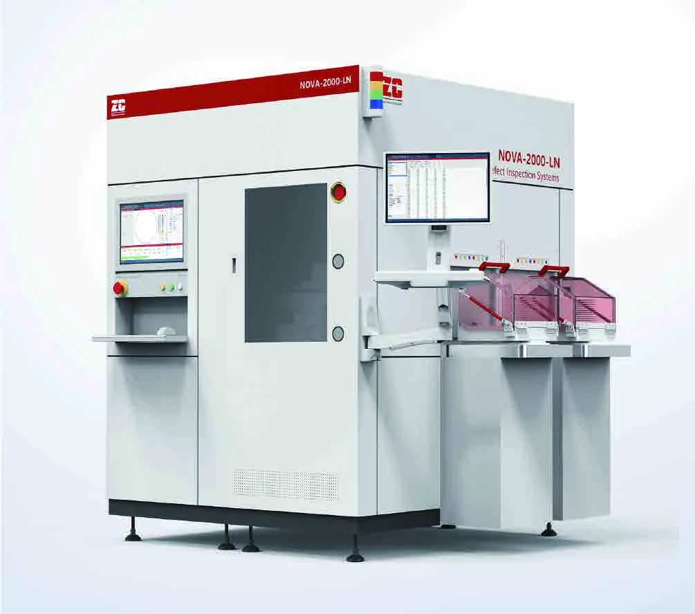
View productDefect inspection for lithium niobate and lithium tantalate substrates.
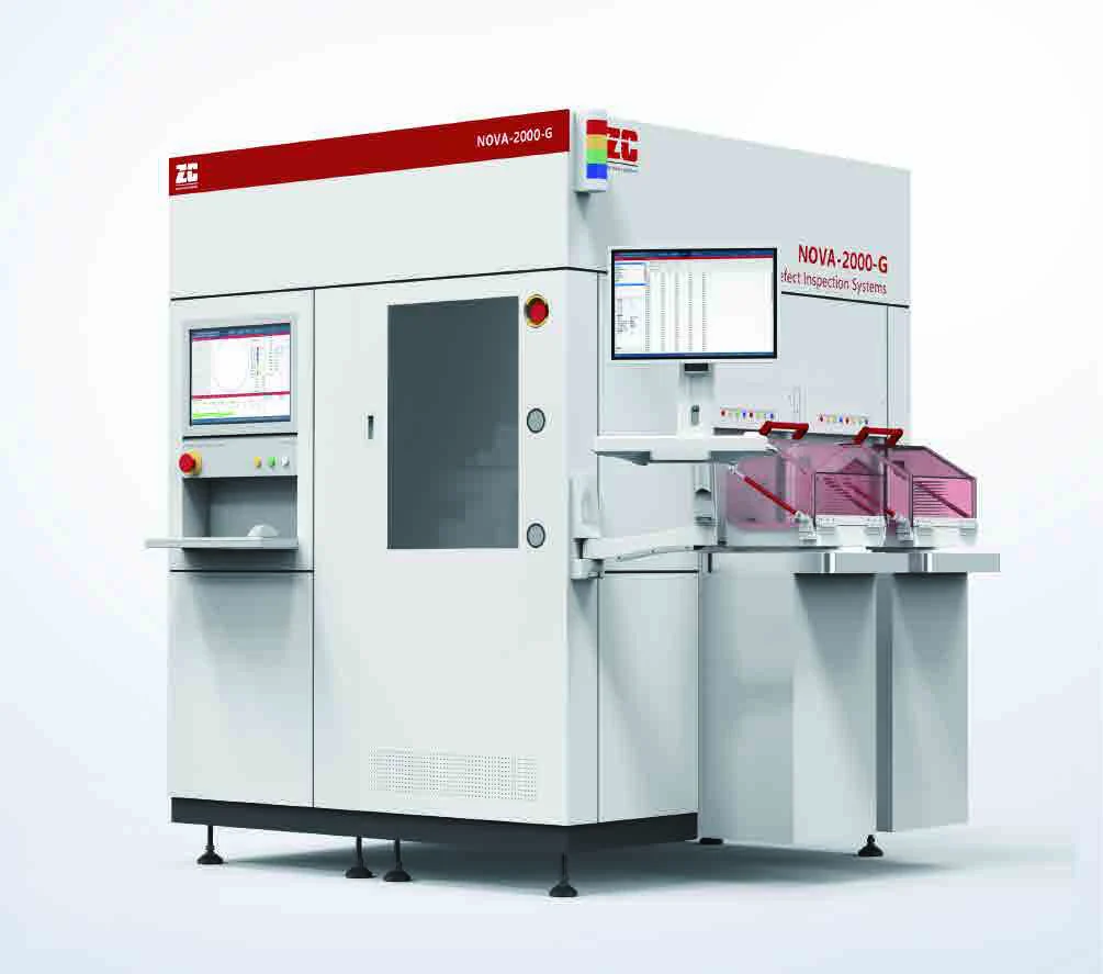
View productOptical defect inspection for glass wafers.
View productPatterned wafer inspection using bright-field, dark-field and differential interference imaging.
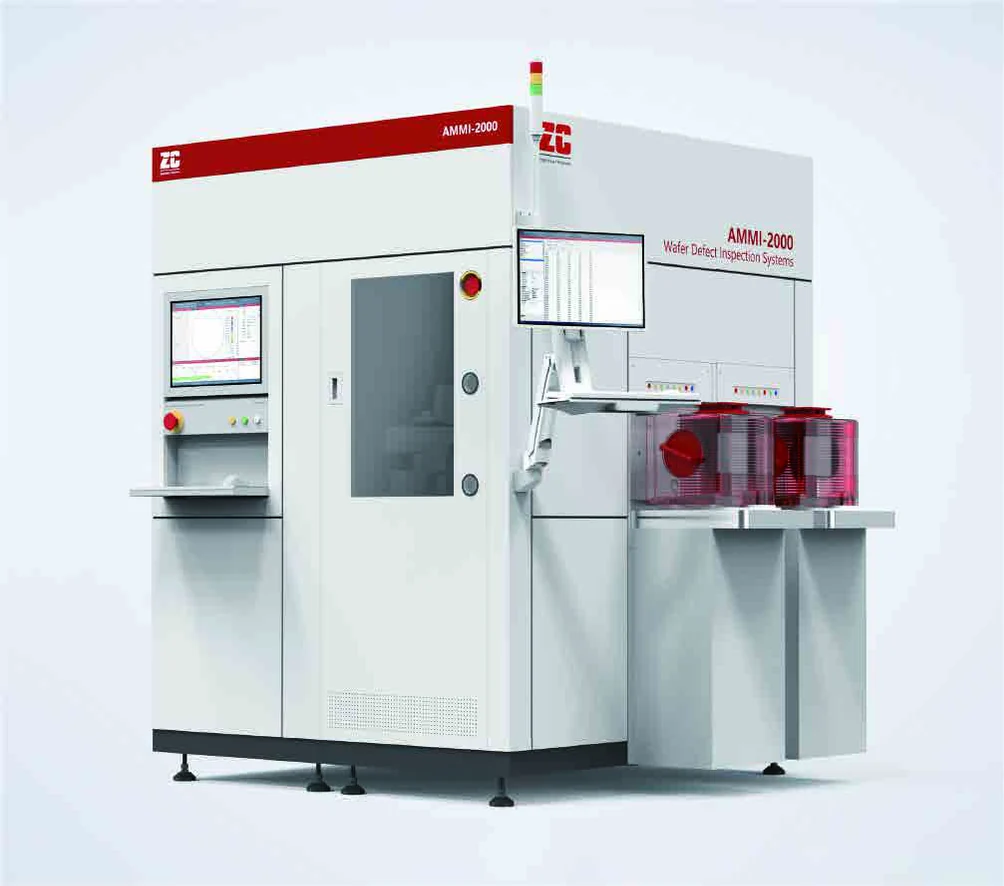
View productOptical wafer defect inspection. Specify wafer material, diameter and target defect size.
View productOptical wafer defect inspection. Specify wafer material, diameter and target defect size.
View productOptical wafer defect inspection. Specify wafer material, diameter and target defect size.
View productAutomated surface defect inspection for precision optical lenses.
View productSurface defect inspection for flat optical elements.
View productAutomated surface defect inspection for optical prisms.
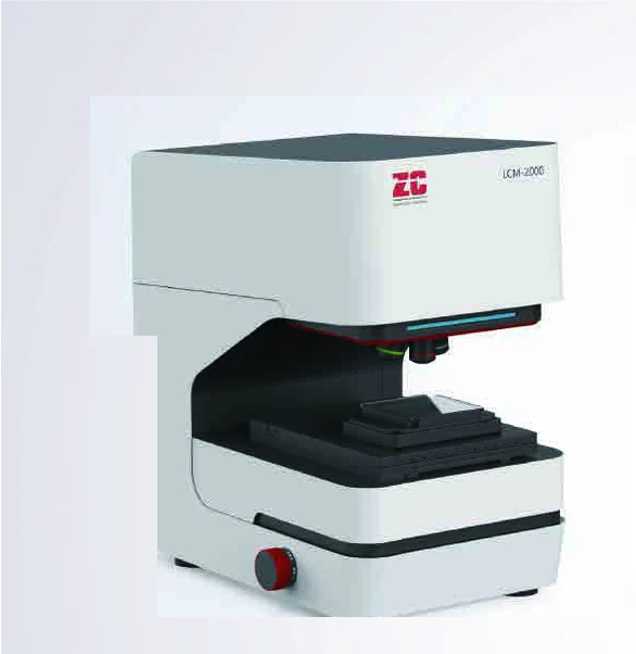
View productNon-contact confocal measurement of microstructure and surface topography.
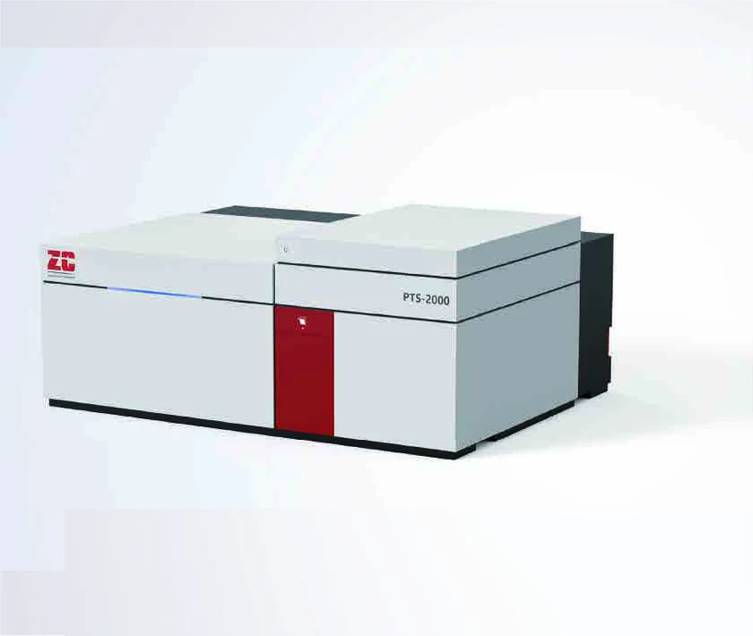
View productPhotothermal measurement of weak optical absorption in substrates and coatings.
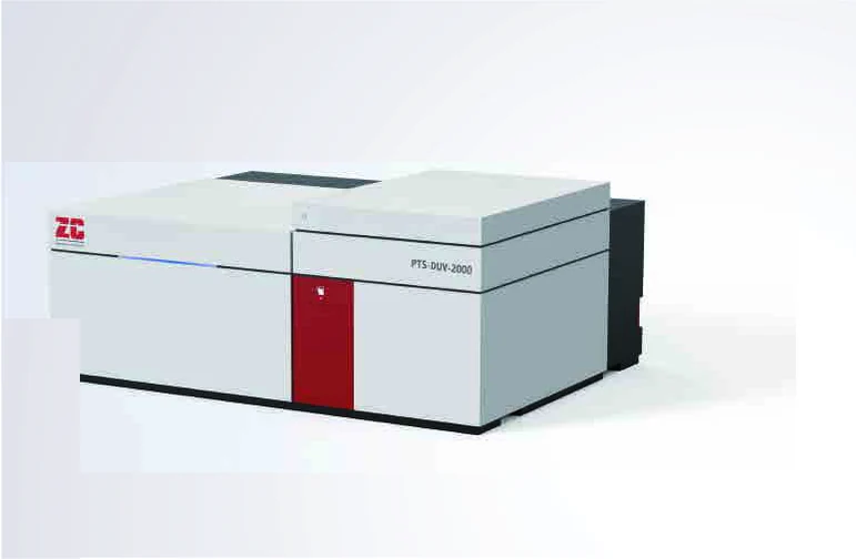
View productDeep-ultraviolet optical absorption measurement for precision optical materials.
View productLaser calorimetry for optical absorption characterization.
View productLaser damage threshold testing and conditioning for optical materials and coatings.
View productMultimodal inspection of surface defects in precision optical components.
View productSurface and subsurface defect inspection for optical materials.
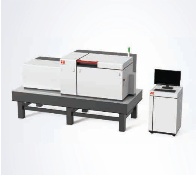
View productLarge-aperture photothermal inspection of optical absorption defects.
View productOptical scattering inspection for large-aperture components.
View productLarge-aperture multimodal optical defect inspection.
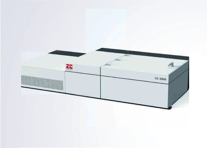
View productTransmittance and reflectance measurement for large-aperture optical components.
View productMeasure thin-film stress on wafers from 100 mm to 300 mm.
View productConfigurable wafer handling with OCR, alignment and double-sided identification.
View productWafer-transfer modules and related equipment support.
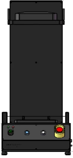
View productAutomatic opening of SMIF reticle pods with selectable RSP150 or RSP200 configuration.
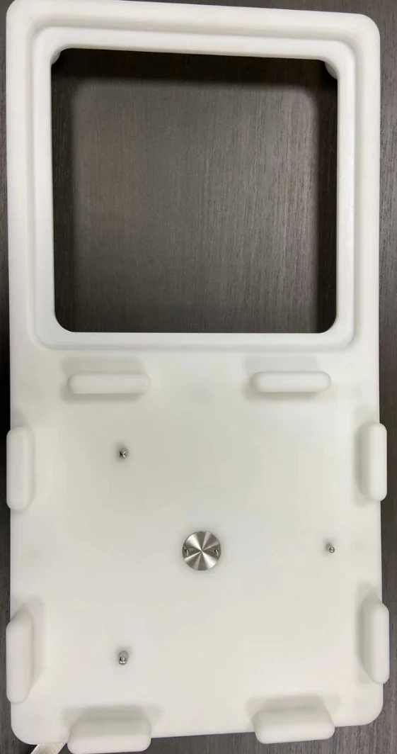
View productManual SMIF reticle pod opening without an electrical supply.
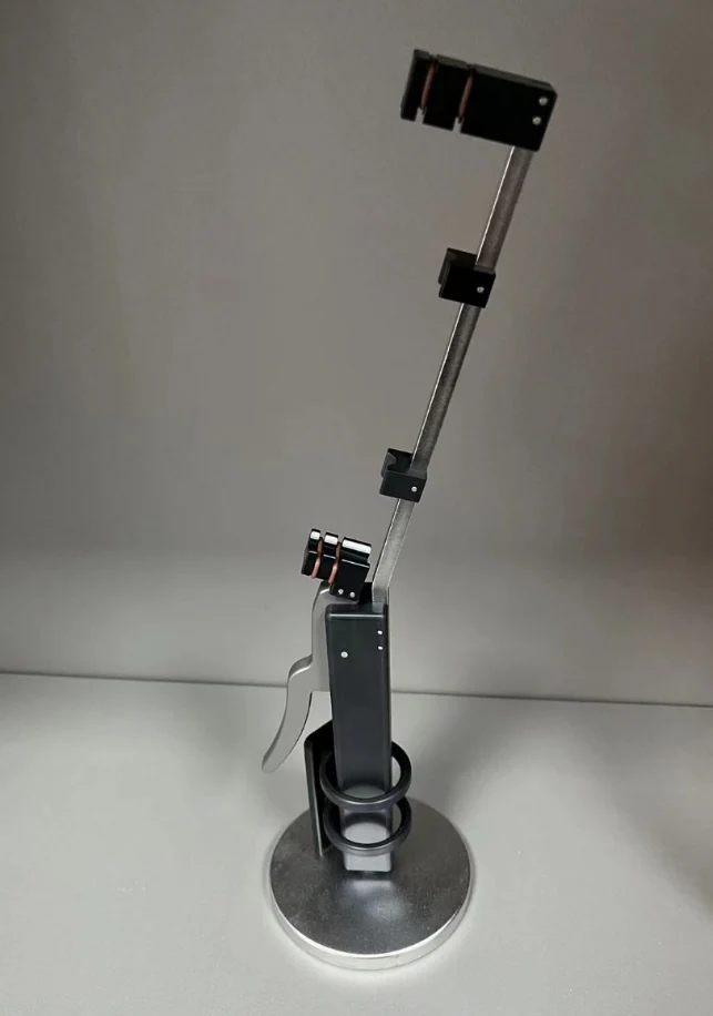
View productF, I and Y reticle grippers for controlled mask handling.
View productLaser Annealing for semiconductor and advanced packaging applications.
View productDevice Laser Annealing for semiconductor and advanced packaging applications.
View productMetrology for semiconductor and advanced packaging applications.
View productStepper for semiconductor and advanced packaging applications.
View productStepper for semiconductor and advanced packaging applications.
View productPackaging AOI for semiconductor and advanced packaging applications.
View product/ SWB Wafer Aligner and Bonder for semiconductor and advanced packaging applications.
View productStepper for semiconductor and advanced packaging applications.
View productManufacturer-stated development platform for compound semiconductor lithography. Confirm current product maturity and configuration.
View productLaser Annealing for semiconductor and advanced packaging applications.
View productLithography scanner for LCD and AMOLED flat-panel display manufacturing.
View productPattern and critical-dimension measurement for display manufacturing.
View productPhotoalignment equipment for IPS TFT-LCD processing.
View productFine-metal-mask tension equipment for AMOLED mask preparation.
View productControl Units for semiconductor and advanced packaging applications.
View productRefurbished mask aligner sourcing and equipment support.
View productRemanufactured equipment family listed in the company portfolio.
View productRemanufactured equipment family listed in the company portfolio.
View productRemanufactured equipment family listed in the company portfolio.
View productRemanufactured equipment family listed in the company portfolio.
View productRemanufactured equipment family listed in the company portfolio.
View productRemanufactured equipment family listed in the company portfolio.
View productLaser cutting and etching system named in the September 2025 portfolio.
View productTry another model or keyword, or ask our team for sourcing support.
Contact our team ↗Products are offered subject to configuration and availability confirmation. Refurbished equipment listings describe sourcing capabilities, not guaranteed current stock.
Share your application, substrate and target specification.